Introduction
P-channel Metal-Oxide-Semiconductor Field-Effect Transistors, or P-channel MOSFETs, are essential elements in electronic circuits, serving vital roles in amplification, switching, and signal processing. This article delves into the core aspects of P-channel MOSFETs, exploring their composition, structure, operation, and distinctive features, while also examining their diverse applications and addressing frequently asked questions.
What is MOSFET ?
A MOSFET, or Metal-Oxide-Semiconductor Field-Effect Transistor, is a type of semiconductor device that plays a crucial role in electronic circuits. It is used for amplifying or switching electronic signals. The MOSFET consists of three main components: a metal gate, an insulating oxide layer (usually made of silicon dioxide), and a semiconductor material (commonly silicon). This arrangement forms a transistor that allows precise control of the flow of electrical current.
What is P Channel MOSFET ?
A P-channel MOSFET, which stands for P-channel Metal-Oxide-Semiconductor Field-Effect Transistor, is a type of metal-oxide-semiconductor field-effect transistor where the majority charge carriers responsible for the flow of electrical current are positive “holes” (absence of electrons). P-channel MOSFETs are fundamental components in electronic circuits, serving various roles such as amplification, switching, and signal processing.
Types of P Channel MOSFET
There are two types of P Channel MOSFETs:
- P Channel Enhancement MOSFET
- P Channel Depletion MOSFET
P Channel MOSFET Symbol
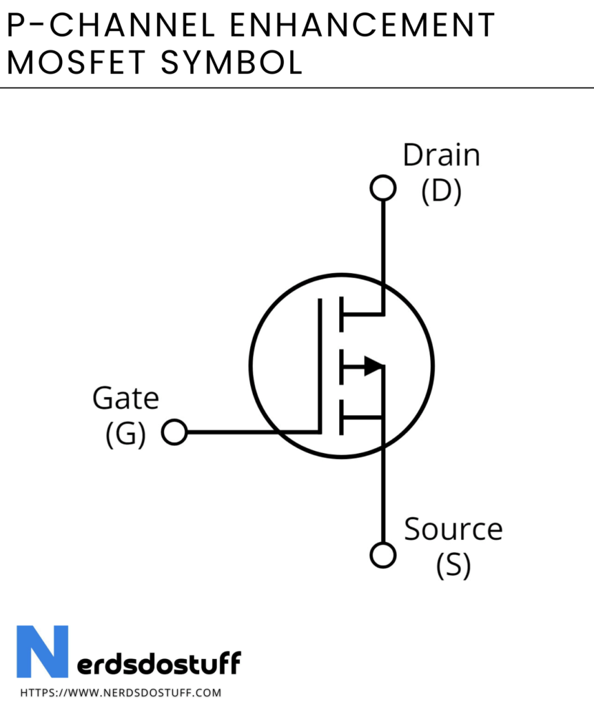
P Channel Enhancement MOSFET symbol

The symbol for a P-channel enhancement-mode MOSFET also consists of three main elements, and here’s a breakdown of each component:
- Arrow Direction:
- Similar to the N-channel MOSFET, the arrow on the symbol points away from the body of the transistor. This arrow indicates the direction of conventional current flow when the transistor is in its active (conducting) state. In the case of a P-channel MOSFET, this direction is opposite to that of an N-channel MOSFET.
- Triangle:
- The triangle in the symbol represents a P-channel MOSFET. However, unlike the N-channel symbol, the arrow is on the side opposite to the source terminal, and the drain terminal is on the side with the arrow. The point of the triangle still represents the gate terminal.
- Arrow on Gate:
- To signify that it is an enhancement-mode MOSFET, there is no line connecting the arrow to the triangle, just like in the N-channel MOSFET symbol. The arrow on the gate indicates that a negative voltage applied to the gate relative to the source enhances the conductivity of the channel, allowing current to flow between the source and drain terminals.
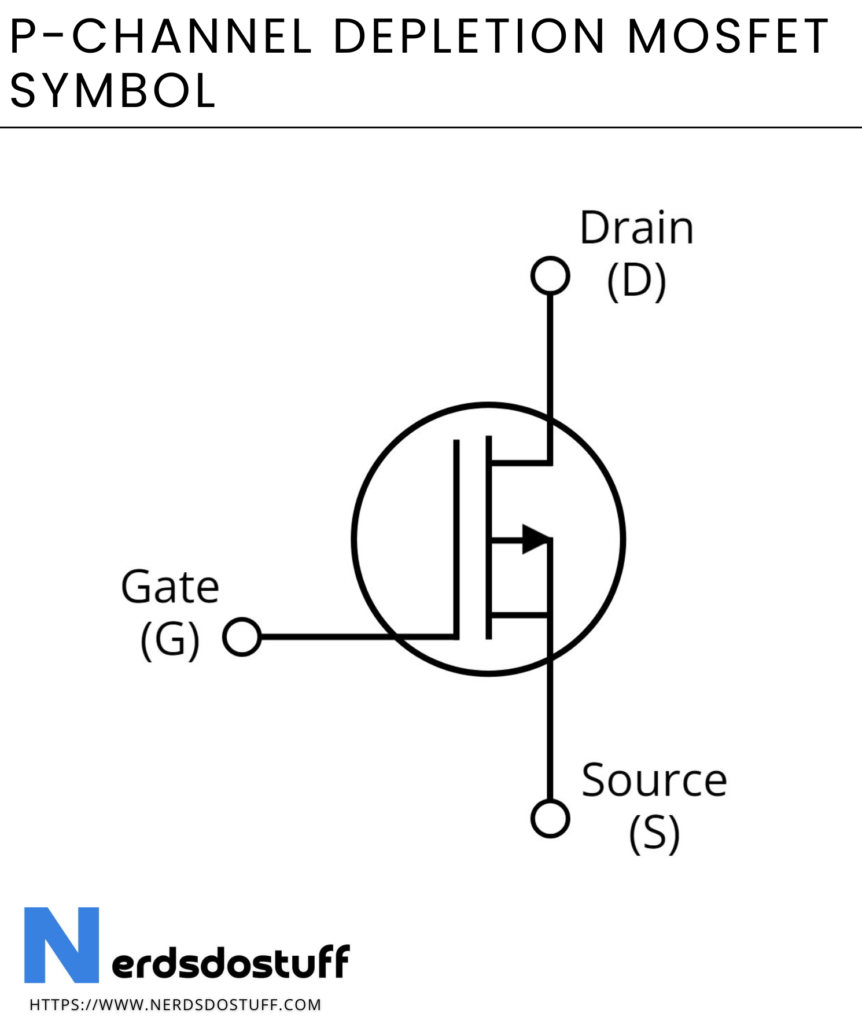
P Channel Depletion MOSFET symbol

The symbol for a P-channel depletion-mode MOSFET consists of three main elements, similar to the enhancement-mode symbol. Here’s a breakdown of each component:
- Arrow Direction:
- As with the enhancement-mode symbol, the arrow points away from the body of the transistor, indicating the direction of conventional current flow when the transistor is in its active (conducting) state. The arrow direction is opposite to that of an N-channel depletion-mode MOSFET.
- Triangle:
- The triangle in the symbol represents a P-channel MOSFET. However, unlike the enhancement-mode symbol, the arrow is on the side opposite to the source terminal, and the drain terminal is on the side with the arrow. The point of the triangle still represents the gate terminal.
- No Arrow on Gate:
- To signify that it is a depletion-mode MOSFET, there is no arrow on the gate in the symbol. In depletion-mode MOSFETs, the channel is normally conducting without an applied voltage, and a more negative voltage on the gate depletes the channel, reducing conductivity.
Construction and Working of P Channel MOSFET
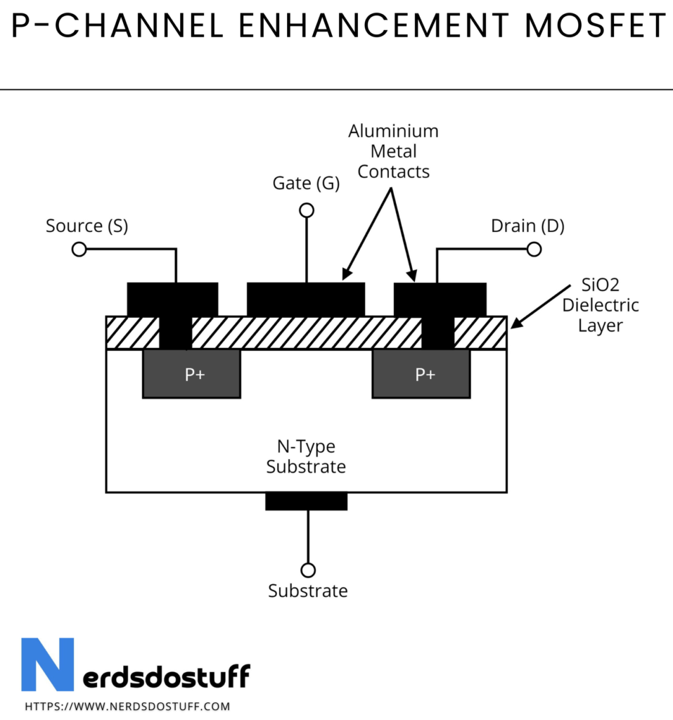
Construction and Working of P Channel Enhancement MOSFET

Construction of N-Channel Enhancement-Mode MOSFET:
The P-channel enhancement-mode MOSFET is constructed using semiconductor materials, typically silicon. The essential components include:
- Substrate: The base material, often made of p-type silicon, serves as the foundation for the MOSFET.
- Source and Drain Regions: N-type doping is used to create the source and drain regions in the silicon substrate. These regions define where current enters (source) and exits (drain) the MOSFET.
- Gate Insulator: A thin insulating layer, usually made of silicon dioxide (SiO2), is deposited over the substrate. This insulator prevents direct electrical contact between the gate and the semiconductor material.
- Metal Gate: A metal layer, often made of aluminum or polysilicon, is deposited on top of the gate insulator. The metal gate is used to control the flow of current between the source and drain regions.
Working of P-Channel Enhancement-Mode MOSFET:
- Off State (No Voltage Applied to Gate):
- In its default or off state, the MOSFET has no conducting channel between the source and drain.
- The absence of voltage on the gate means there is no electric field to induce a channel.
- Applying a Negative Voltage to the Gate:
- When a negative voltage is applied to the gate relative to the source (Vgs), an electric field is created.
- This electric field attracts positive holes from the P-type source region towards the insulating oxide layer.
- Formation of Conducting Channel:
- With a sufficiently negative Vgs, the electric field causes the positive holes to accumulate just beneath the oxide layer, forming a conductive channel between the source and drain.
- This conducting channel allows current to flow from the source to the drain terminals.
- On State (Conduction):
- The MOSFET is now in its on state, conducting current between the source and drain.
- The conductivity of the channel is directly proportional to the magnitude of the applied gate-source voltage.
- Off State (No Voltage or Low Voltage on the Gate):
- If the gate voltage is reduced or returned to zero, the conducting channel gradually disappears, and the MOSFET returns to its off state.
- The MOSFET remains in the off state until a negative voltage is reapplied to the gate.
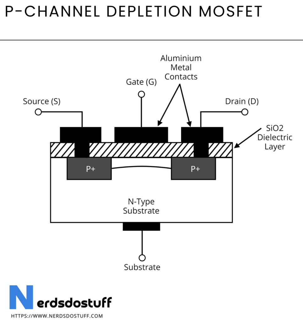
Construction and Working of P Channel Depletion MOSFET

Construction of P-Channel Depletion-Mode MOSFET:
The P-channel depletion-mode MOSFET is constructed using semiconductor materials, typically silicon. The main components include:
- Substrate: The substrate serves as the base material, often made of p-type silicon, providing the foundation for the MOSFET.
- Source and Drain Regions: N-type doping is used to create the source and drain regions in the silicon substrate, defining where current enters (source) and exits (drain) the MOSFET.
- Gate Insulator: Similar to the enhancement-mode MOSFET, a thin insulating layer, usually made of silicon dioxide (SiO2), is deposited over the substrate. This layer prevents direct electrical contact between the gate and the semiconductor material.
- Metal Gate: A metal layer, often made of aluminum or polysilicon, is deposited on top of the gate insulator. The metal gate is used to control the flow of current between the source and drain regions.
Working of P-Channel Depletion-Mode MOSFET:
- Default State (No Voltage Applied to Gate):
- In its default state, the MOSFET has a conducting channel between the source and drain.
- This is because the depletion-mode MOSFET is normally “on” without the application of an external voltage.
- Applying a Positive Voltage to the Gate (Reverse Bias):
- Unlike the enhancement-mode MOSFET, the depletion-mode MOSFET operates with a positive voltage applied to the gate relative to the source (Vgs).
- The positive gate voltage creates an electric field that attracts free electrons from the N-type channel, depleting the channel of charge carriers.
- Reduction of Conducting Channel:
- As the positive gate voltage increases, more electrons are drawn away from the channel, reducing its conductivity.
- This reduction continues until the channel is nearly depleted of free charge carriers.
- Off State (High Positive Voltage on the Gate):
- With a sufficiently positive Vgs, the conducting channel becomes depleted, and the MOSFET transitions to its off state.
- In this off state, the MOSFET exhibits high resistance, preventing significant current flow between the source and drain terminals.
- On State (Zero or Low Positive Voltage on the Gate):
- If the positive gate voltage is reduced or returned to zero, the free electrons return to the channel, allowing it to conduct current.
- The MOSFET is now in its on state, and the conductivity of the channel is restored.
Applications of P Channel MOSFET
- Power Management:
- P-channel MOSFETs are frequently used in power management circuits, such as voltage regulators and battery protection circuits. Their ability to handle higher voltage levels and moderate currents makes them suitable for efficiently controlling and regulating power in electronic devices.
- Audio Amplifiers:
- P-channel MOSFETs play a crucial role in audio amplifier circuits, particularly in the output stages. They are employed to amplify audio signals with high fidelity and efficiency. Their characteristics make them suitable for driving speakers and other audio devices.
- Switch-Mode Power Supplies (SMPS):
- In switch-mode power supply circuits, P-channel MOSFETs are utilized to control the switching action in the power supply. Their high voltage-handling capability and efficient switching properties contribute to the overall performance and energy efficiency of SMPS.
- LED Drivers:
- P-channel MOSFETs are used in LED driver circuits to regulate and control the current flowing through Light Emitting Diodes (LEDs). They play a vital role in achieving precise control over the brightness of LEDs in various lighting applications.
- Complementary Metal-Oxide-Semiconductor (CMOS) Technology:
- P-channel MOSFETs are an integral part of CMOS technology, where they work in conjunction with N-channel MOSFETs to form complementary pairs. CMOS technology is widely used in integrated circuits, such as microprocessors, memory chips, and digital logic circuits, due to its low power consumption and high noise margins.
FAQs
Q. How does a P-channel MOSFET differ from an N-channel MOSFET?
P-channel and N-channel MOSFETs differ primarily in the type of charge carriers they use for conduction. P-channel MOSFETs utilize positive charge carriers (holes), while N-channel MOSFETs use negative charge carriers (electrons). Understanding these differences is crucial for selecting the appropriate MOSFET for a given application.
Q. What is the significance of the arrow direction in the symbol of a P-channel MOSFET?
The arrow in the symbol of a P-channel MOSFET indicates the direction of conventional current flow when the transistor is in its active (conducting) state. The arrow points away from the body of the transistor, helping engineers and technicians understand the direction of current flow during circuit analysis and design.
Q: How is a P-channel MOSFET turned on and off?
A P-channel MOSFET is turned on when a negative voltage is applied to the gate relative to the source terminal (Vgs < 0). This creates an electric field that enhances the conductivity of the channel, allowing current to flow. Conversely, turning off the P-channel MOSFET involves reducing the negative voltage on the gate or returning it to zero (Vgs ≥ 0), depleting the channel and restricting current flow.
Q: What are common applications for P-channel MOSFETs?
P-channel MOSFETs are widely used in applications such as power management, audio amplifiers, switch-mode power supplies (SMPS), LED drivers, and complementary metal-oxide-semiconductor (CMOS) technology. Understanding these applications helps in selecting the right MOSFET for specific design requirements.
Q: How do P-channel MOSFETs contribute to power efficiency in electronic circuits?
P-channel MOSFETs contribute to power efficiency by efficiently controlling the flow of electrical current in various applications. Their characteristics, such as high input impedance and low ON resistance, make them suitable for minimizing power losses in power management circuits, amplifiers, and other energy-sensitive systems.
Q. What precautions should be taken when using P-channel MOSFETs in electronic designs?
Designers should be aware of voltage ratings, current-carrying capacities, and heat dissipation considerations when using P-channel MOSFETs. Adhering to datasheet specifications, avoiding overvoltage conditions, and implementing proper heat sinking are crucial for ensuring the reliability and longevity of P-channel MOSFETs in electronic circuits.
