Introduction
Depletion MOSFETs play a crucial role in boosting signals and managing the flow of electricity. If you’ve ever been curious about how your gadgets actually work, these components are the key players. In this article, we’ll learn the basics of Depletion MOSFETs – from what they’re made of, their construction, working and characteristics. We will also learn where these MOSFETs are used and answer some FAQs.
What is Depletion MOSFET ?
Depletion MOSFET, or Depletion Mode Metal-Oxide-Semiconductor Field-Effect Transistor, operates with a conductive channel in its default state. Unlike Enhancement MOSFETs, which require an external voltage to enhance conductivity, Depletion MOSFETs possess an intrinsic conductive channel that can be depleted by applying a voltage.
Types of Depletion MOSFET
There are two types of Depletion MOSFETs:
- N Channel Depletion MOSFET
- P Channel Depletion MOSFET
Symbols of Depletion MOSFET
N Channel Depletion MOSFET symbol
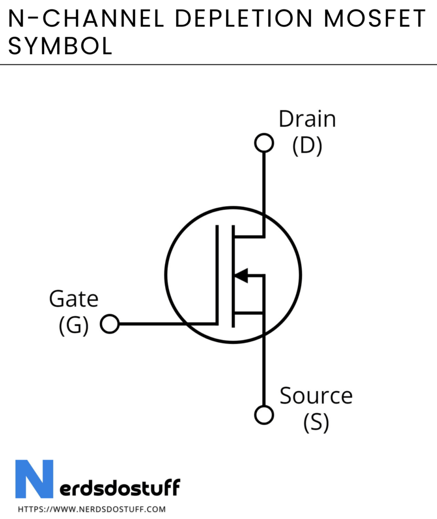
N Channel Depletion MOSFETs employ an N-type semiconductor as the channel. The symbol depicts an arrow pointing inward, indicating the default flow of current from drain to source when no external voltage is applied.
P Channel Depletion MOSFET symbol
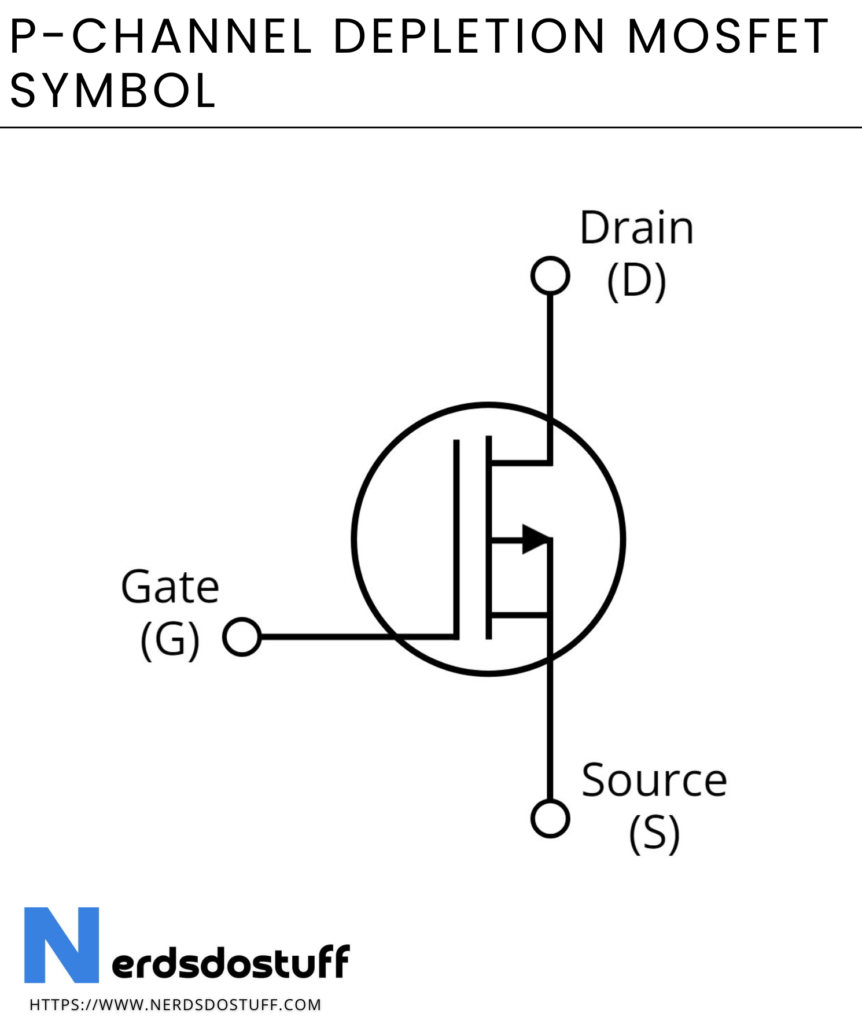
Conversely, P Channel Depletion MOSFETs feature a P-type semiconductor channel. The symbol showcases an arrow pointing outward, signifying the default current flow from source to drain without external voltage application.
Construction and Working of Depletion MOSFET
Depletion MOSFETs share some similarities with their Enhancement MOSFET counterparts in terms of basic structure. The device consists of three main regions – source, drain, and a channel. The channel is typically made of either N-type or P-type semiconductor material, depending on whether it’s an N Channel or P Channel Depletion MOSFET.
Construction of N Channel Depletion MOSFET
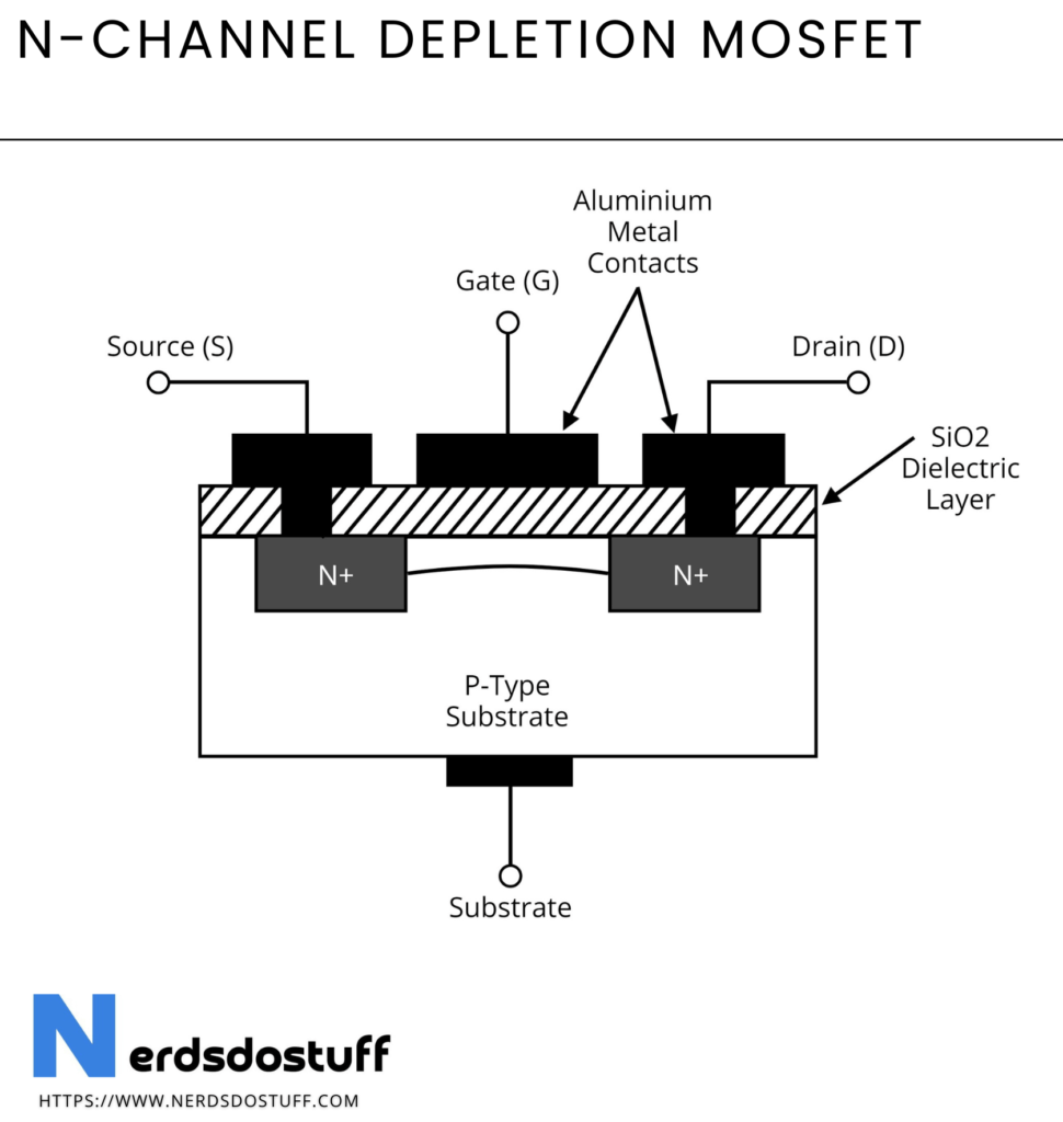
- Default Conductive Channel: Unlike Enhancement MOSFETs, Depletion MOSFETs have an intrinsic conductive channel even when no external voltage is applied. This default conductivity is due to the naturally occurring charge carriers in the channel.
- Application of External Voltage: When a negative voltage is applied to the gate relative to the source, it induces an electric field that depletes the charge carriers in the channel. This depletion creates a “pinch-off” region, restricting the flow of current between the source and drain.
- Controlled Current Flow: By adjusting the gate-source voltage, the width of the conductive channel is controlled, regulating the flow of charge carriers. This controlled modulation of the channel’s conductivity allows for precise management of current flow, making the N Channel Depletion MOSFET a versatile component in various electronic circuits.
Construction of P Channel Depletion MOSFET
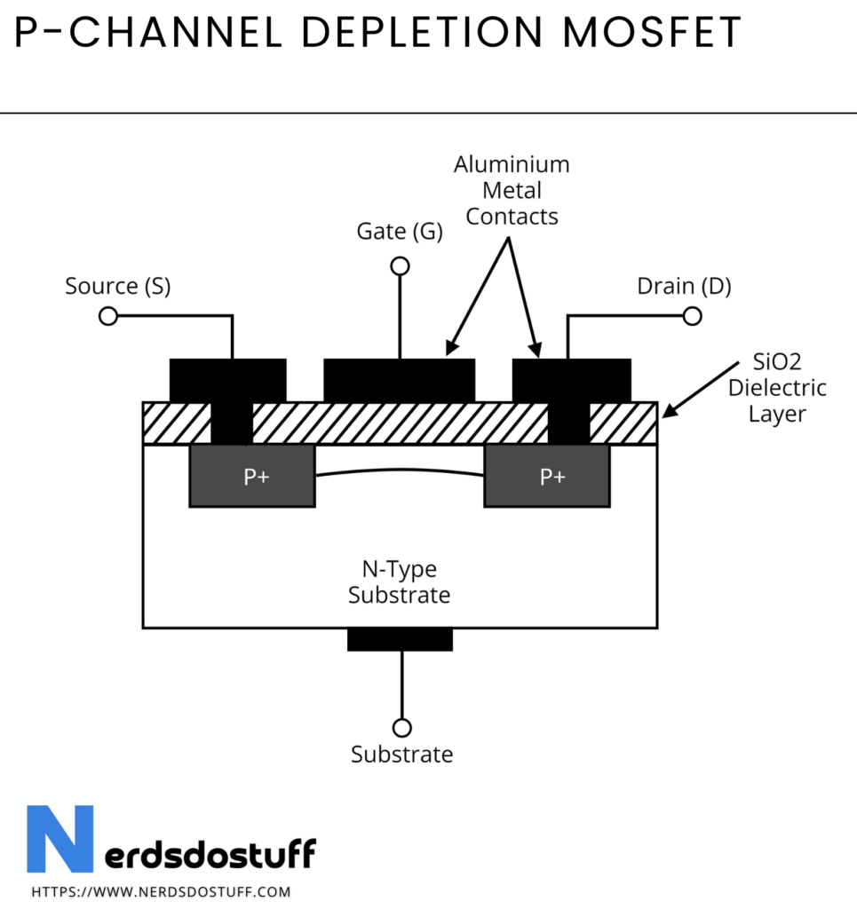
- Default Conductive Channel: Similar to the N Channel counterpart, the P Channel Depletion MOSFET has an intrinsic conductive channel in its default state. The channel conducts current between the source and drain without the need for an external voltage.
- Application of External Voltage: Applying a positive voltage to the gate relative to the source induces an electric field that depletes charge carriers in the channel, creating a pinch-off region. This depletion controls the width of the conductive channel, regulating the current flow between the source and drain.
- Precise Current Regulation: By manipulating the gate-source voltage, the P Channel Depletion MOSFET achieves controlled modulation of the channel’s conductivity, allowing for accurate regulation of current flow. This characteristic makes it a valuable component in applications where precise current control is essential.
Characteristics of Depletion MOSFET
Transfer and Drain Characteristics of N Channel Depletion MOSFET
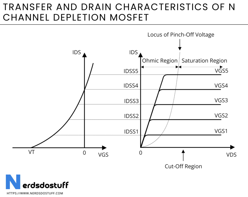
The transfer characteristics of an N Channel Depletion MOSFET illustrate the relationship between the gate-source voltage (VGS) and the resulting drain current (ID).
- Forward Bias (Negative VGS): In the forward bias region, where VGS is negative, the MOSFET operates with a naturally conductive channel. As VGS becomes more negative, the depletion region widens, reducing the conductive channel’s width and, consequently, the drain current (ID).
- Threshold Voltage (Vth): The threshold voltage is the point at which the MOSFET transitions from the naturally conductive state to the pinched-off state. It signifies the minimum VGS required to control the channel.
- Pinched-Off Region: As VGS continues to become more negative, the MOSFET enters the pinched-off region. In this region, the channel is depleted, and ID is significantly reduced.
The drain characteristics of an N Channel Depletion MOSFET depict the relationship between the drain-source voltage (VDS) and the resulting drain current (ID), with the gate-source voltage (VGS) as a parameter.
- Saturation Region: In the saturation region, where VDS is relatively small, ID remains relatively constant. The MOSFET operates with a saturated, fully open channel.
- Triode (or Ohmic) Region: As VDS increases, the MOSFET enters the triode region, where ID is linearly dependent on VDS. The channel is partially pinched off, and the MOSFET acts as a variable resistor.
- Cutoff Region: At higher VDS, the MOSFET enters the cutoff region, and ID becomes almost independent of VDS. The channel is fully pinched off, and the MOSFET behaves like an open switch.
Transfer and Drain Characteristics of P Channel Depletion MOSFET
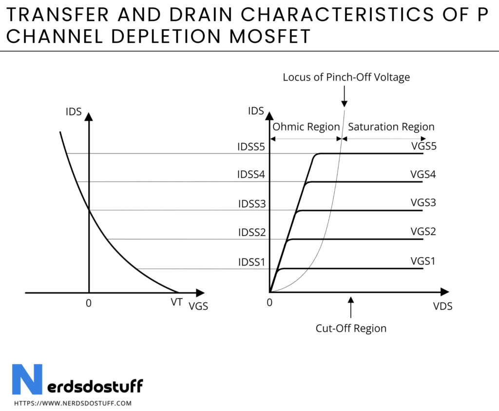
The transfer characteristics of a P Channel Depletion MOSFET show the relationship between the gate-source voltage (VGS) and the resulting drain current (ID).
- Forward Bias (Positive VGS): In the forward bias region, where VGS is positive, the MOSFET operates with a naturally conductive channel. As VGS becomes more positive, the depletion region widens, reducing the conductive channel’s width and, consequently, the drain current (ID).
- Threshold Voltage (Vth): Similar to the N Channel case, the threshold voltage is the point at which the MOSFET transitions from the naturally conductive state to the pinched-off state.
- Pinched-Off Region: As VGS continues to become more positive, the MOSFET enters the pinched-off region, where the channel is depleted, and ID decreases significantly.
The drain characteristics of a P Channel Depletion MOSFET show the relationship between the drain-source voltage (VDS) and the resulting drain current (ID), with the gate-source voltage (VGS) as a parameter.
- Saturation Region: In the saturation region, where VDS is relatively small, ID remains relatively constant. The MOSFET operates with a saturated, fully open channel.
- Triode (or Ohmic) Region: As VDS increases, the MOSFET enters the triode region, where ID is linearly dependent on VDS. The channel is partially pinched off, and the MOSFET acts as a variable resistor.
- Cutoff Region: At higher VDS, the MOSFET enters the cutoff region, and ID becomes almost independent of VDS. The channel is fully pinched off, and the MOSFET behaves like an open switch.
Applications of Depletion MOSFET
Voltage-Level Shifting: Depletion MOSFETs are commonly used in circuits where voltage-level shifting is required. Their inherent conductivity allows them to serve as efficient level shifters, enabling the translation of signals between different voltage levels without the need for additional components. This application is particularly useful in interfacing digital circuits operating at different voltage levels, ensuring seamless communication between various parts of a system.
Analog Switching Circuits: Depletion MOSFETs find extensive use in analog switching circuits due to their ability to provide precise control over current flow. These MOSFETs act as reliable switches, allowing analog signals to be routed or switched between different paths within a circuit. Their inherent conductivity and ability to modulate current make them ideal for applications requiring accurate and controlled switching, such as audio signal routing and analog multiplexing.
Current Limiters: Depletion MOSFETs are employed as current limiters in specific circuit configurations where precise current control is essential. By adjusting the gate-source voltage, the conductivity of the MOSFET’s channel can be modulated to limit the amount of current flowing through a circuit. This application is particularly useful in protecting sensitive components from excessive current and ensuring the stability and reliability of electronic systems, such as in overcurrent protection circuits and battery management systems.
Amplifiers: Depletion MOSFETs are also used in certain amplifier circuits where their inherent conductivity and ability to modulate current play a crucial role. These MOSFETs can be employed as active elements in amplifier stages, allowing for the amplification of analog signals with minimal distortion. Their precise control over current flow enables the design of high-performance amplifiers capable of accurately reproducing input signals with minimal noise and distortion, making them suitable for applications such as audio amplification and instrumentation amplifiers.
Digital Logic Circuits: While less common than Enhancement MOSFETs, Depletion MOSFETs can also be utilized in certain digital logic circuits where their unique characteristics are advantageous. These MOSFETs can serve as active elements in logic gates, allowing for the implementation of specific logic functions within a digital circuit. Their inherent conductivity and ability to modulate current make them suitable for applications where low-power consumption and precise signal processing are paramount, such as in low-power digital logic circuits and mixed-signal integrated circuits.
FAQs
Q. What distinguishes Depletion MOSFETs from Enhancement MOSFETs?
While both types of MOSFETs share similarities, the key distinction lies in their default states. Depletion MOSFETs have a naturally conductive channel even without an applied voltage, in contrast to Enhancement MOSFETs, which require an external voltage to create a conductive channel.
Q. How does a Depletion MOSFET function as a current limiter?
Depletion MOSFETs can act as current limiters by modulating the conductivity of their intrinsic channel. Adjusting the gate-source voltage allows precise control over the channel’s width, effectively limiting the current flowing through the circuit. This feature is crucial for protecting components from excessive current in various applications.
Q: In what scenarios are Depletion MOSFETs preferred over Enhancement MOSFETs?
Depletion MOSFETs are preferred in applications where a default conductive channel is advantageous. They find use in circuits requiring voltage-level shifting, analog switching, and precise current control. Additionally, their unique characteristics make them suitable for specific amplifier and digital logic circuit configurations.
Q: How do Depletion MOSFETs contribute to analog signal processing?
Depletion MOSFETs play a significant role in analog signal processing due to their ability to provide accurate and controlled current modulation. In amplifier circuits, they contribute to the amplification of analog signals with minimal distortion, making them valuable components in applications such as audio amplifiers and instrumentation amplifiers.
Q: Can Depletion MOSFETs be used in digital logic circuits?
Yes, Depletion MOSFETs can be utilized in certain digital logic circuits where their inherent conductivity and modulation capabilities offer advantages. They may serve as active elements in logic gates, particularly in applications requiring low-power consumption and precise signal processing, such as in low-power digital logic circuits and mixed-signal integrated circuits.
Q: How are Depletion MOSFETs employed in voltage-level shifting?
In voltage-level shifting applications, Depletion MOSFETs capitalize on their default conductive channel. By adjusting the gate-source voltage, they enable seamless translation of signals between different voltage levels without the need for additional components. This makes them valuable in interfacing digital circuits operating at varying voltage levels within a system.
