Introduction
Enhancement MOSFETs play a crucial role in boosting signals and managing the flow of electricity. If you’ve ever been curious about how your gadgets actually work, these components are the key players. In this article, we’ll learn the basics of Enhancement MOSFETs – from what they’re made of, their construction, working and characteristics. We will also learn where these MOSFETs are used and answer some FAQs.
What is Enhancement MOSFET ?
MOSFET, or Metal-Oxide-Semiconductor Field-Effect Transistor, is a fundamental component in electronic circuits. Enhancement MOSFETs, a subtype of MOSFETs, excel in amplifying weak signals and efficiently regulating current flow. Unlike their depletion counterparts, Enhancement MOSFETs require an external voltage to enhance conductivity.
Types of Enhancement MOSFET
There are two types of Enhancement MOSFETs:
- N Channel Enhancement MOSFET
- P Channel Enhancement MOSFET
Symbols of Enhancement MOSFET
N Channel Enhancement MOSFET symbol
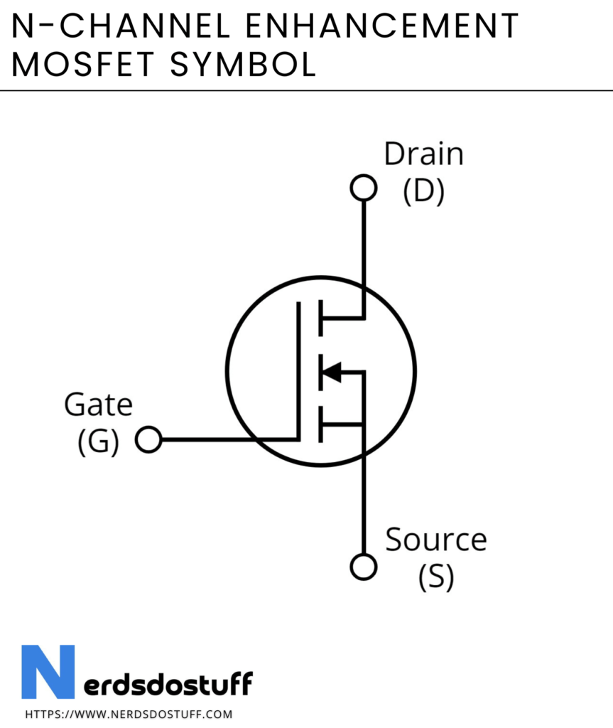
N Channel Enhancement MOSFETs are characterized by the presence of an N-type semiconductor as the channel. The symbol comprises an arrow pointing outwards from the transistor, representing the direction of current flow when a positive voltage is applied, allowing electrons to flow from the source to the drain through the N-type channel.
P Channel Enhancement MOSFET symbol
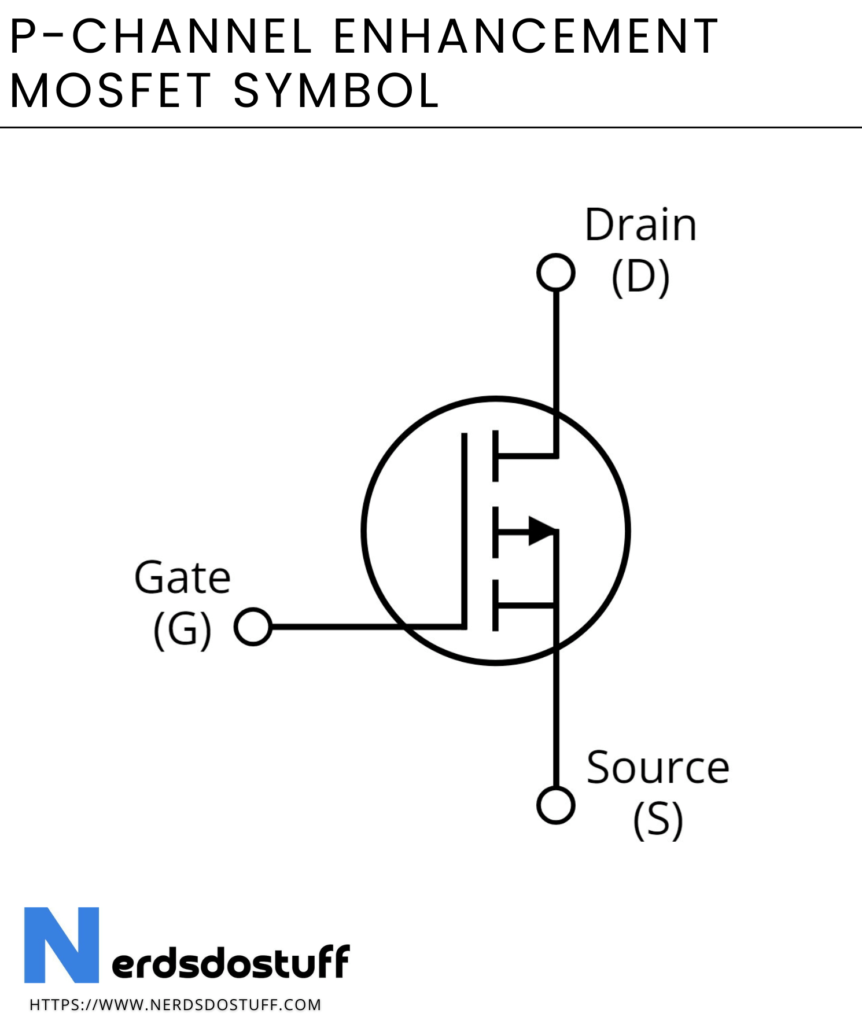
Conversely, P Channel Enhancement MOSFETs employ a P-type semiconductor for the channel. The symbol features an arrow pointing inwards, denoting the direction of current flow when a negative voltage is applied, enabling holes to move from the source to the drain through the P-type channel.
Construction and Working of Enhancement MOSFET
Construction of N Channel Enhancement MOSFET
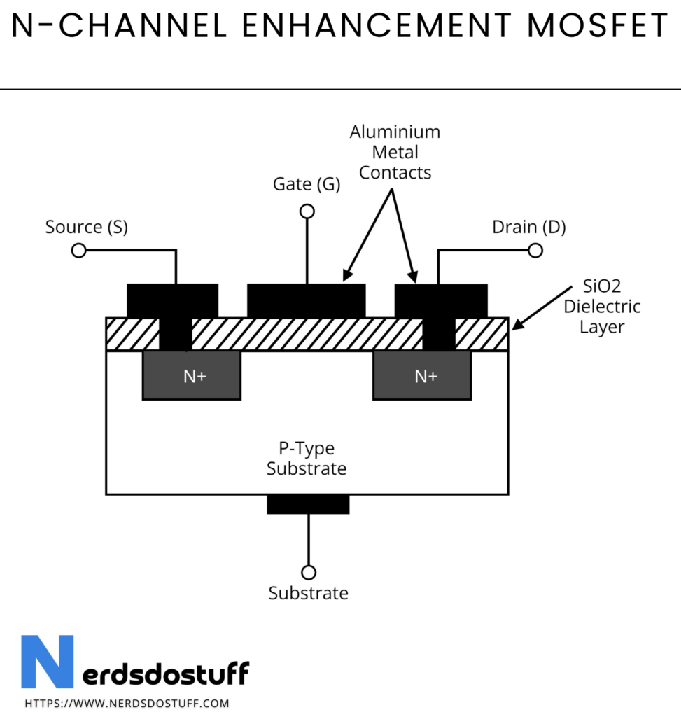
The N Channel Enhancement MOSFET is a semiconductor device constructed with an N-type material serving as the channel. This channel is created within a P-type substrate, forming a P-N junction. The structure also includes a thin layer of insulating material (usually silicon dioxide) known as the gate oxide, which separates the gate terminal from the channel.
When a positive voltage is applied to the gate terminal relative to the source terminal, it creates an electric field across the gate oxide. This electric field attracts free electrons from the N-type channel towards the gate, forming a conductive channel between the source and drain terminals. As the gate voltage increases, the conductivity of the channel enhances, allowing more electrons to flow from the source to the drain.
This modulation of conductivity enables the N Channel Enhancement MOSFET to amplify weak input signals. By controlling the gate-source voltage, the device can regulate the flow of electrons through the channel, thus controlling the output current.
Construction of P Channel Enhancement MOSFET
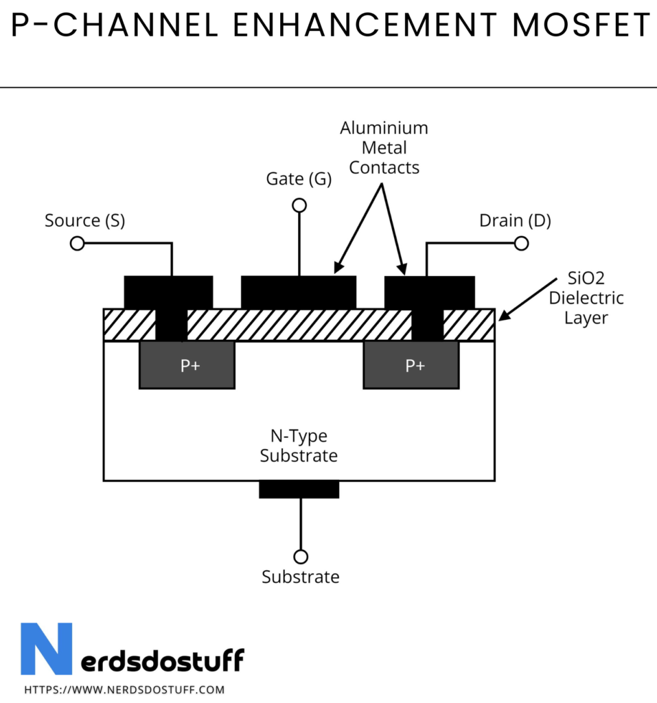
The P Channel Enhancement MOSFET utilizes a P-type semiconductor channel within an N-type substrate. Similar to the N Channel MOSFET, it also features a gate oxide layer separating the gate terminal from the channel.
When a negative voltage is applied to the gate terminal relative to the source terminal, it creates an electric field across the gate oxide. This electric field attracts positively charged holes from the P-type channel towards the gate, forming a conductive channel between the source and drain terminals. As the gate voltage becomes more negative, the conductivity of the channel enhances, allowing more holes to flow from the source to the drain.
This controlled modulation of conductivity enables the P Channel Enhancement MOSFET to efficiently regulate current flow. By adjusting the gate-source voltage, the device can control the flow of holes through the channel, thus controlling the output current.
Characteristics of Enhancement MOSFET
Transfer and Drain Characteristics of N Channel Enhancement MOSFET
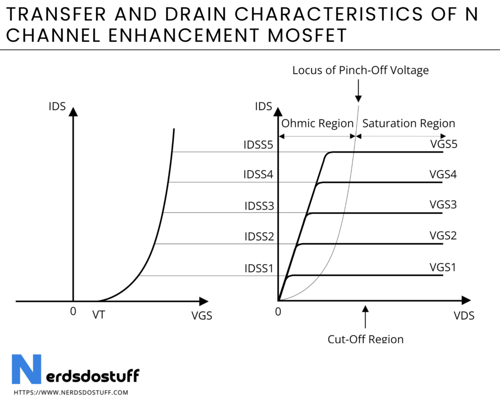
The transfer characteristics of an N Channel Enhancement MOSFET depict the relationship between the gate-source voltage (VGS) and the resulting drain current (ID).
- Forward Bias (Positive VGS): In the forward bias region, where VGS is positive, the MOSFET operates with a minimal conductive channel. As VGS becomes more positive, the conductive channel widens, allowing an increase in the drain current (ID).
- Threshold Voltage (Vth): The threshold voltage is the minimum VGS required to create a conductive channel. Below this threshold, the MOSFET remains in a non-conductive state.
- Enhancement Region: As VGS continues to become more positive beyond the threshold voltage, the MOSFET enters the enhancement region. In this region, the conductive channel is fully established, and ID increases proportionally with VGS.
The drain characteristics of an N Channel Enhancement MOSFET depict the relationship between the drain-source voltage (VDS) and the resulting drain current (ID), with the gate-source voltage (VGS) as a parameter.
- Saturation Region: In the saturation region, where VDS is relatively small, the MOSFET operates with a fully open channel, and ID remains relatively constant.
- Triode (or Ohmic) Region: As VDS increases, the MOSFET enters the triode region, where ID is linearly dependent on VDS. The channel is partially pinched off, and the MOSFET acts as a variable resistor.
- Cutoff Region: At higher VDS, the MOSFET enters the cutoff region, and ID becomes almost independent of VDS. The channel is fully pinched off, and the MOSFET behaves like an open switch.
Transfer and Drain Characteristics of P Channel Enhancement MOSFET
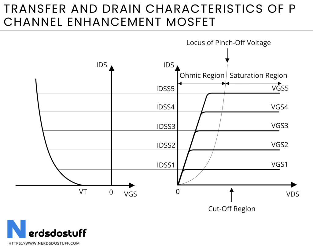
The transfer characteristics of a P Channel Enhancement MOSFET show the relationship between the gate-source voltage (VGS) and the resulting drain current (ID).
- Forward Bias (Negative VGS): In the forward bias region, where VGS is negative, the MOSFET operates with a minimal conductive channel. As VGS becomes more negative, the conductive channel widens, allowing an increase in the drain current (ID).
- Threshold Voltage (Vth): Similar to the N Channel case, the threshold voltage is the minimum VGS required to create a conductive channel. Below this threshold, the MOSFET remains in a non-conductive state.
- Enhancement Region: As VGS continues to become more negative beyond the threshold voltage, the MOSFET enters the enhancement region. In this region, the conductive channel is fully established, and ID increases proportionally with VGS.
The drain characteristics of a P Channel Enhancement MOSFET show the relationship between the drain-source voltage (VDS) and the resulting drain current (ID), with the gate-source voltage (VGS) as a parameter.
- Saturation Region: In the saturation region, where VDS is relatively small, the MOSFET operates with a fully open channel, and ID remains relatively constant.
- Triode (or Ohmic) Region: As VDS increases, the MOSFET enters the triode region, where ID is linearly dependent on VDS. The channel is partially pinched off, and the MOSFET acts as a variable resistor.
- Cutoff Region: At higher VDS, the MOSFET enters the cutoff region, and ID becomes almost independent of VDS. The channel is fully pinched off, and the MOSFET behaves like an open switch.
Applications of Enhancement MOSFET
- Amplifiers: MOSFETs play a crucial role in amplifiers by controlling the flow of current through the circuit. They are used to amplify weak input signals by modulating the conductivity of the channel based on the applied gate-source voltage. This allows for the amplification of signals with minimal distortion, making MOSFETs ideal for use in audio amplifiers, operational amplifiers, and RF amplifiers.
- Switching Circuits: MOSFETs are widely used in switching circuits for their ability to rapidly switch between ON and OFF states. By applying an appropriate gate-source voltage, MOSFETs can control the flow of current through the circuit, making them essential components in power switches, motor control circuits, and digital logic gates. Their fast switching speed and low ON-state resistance make them ideal for high-frequency switching applications.
- Voltage Regulators: MOSFETs are commonly used in voltage regulator circuits to regulate and stabilize the output voltage. By controlling the conductivity of the channel, MOSFETs can adjust the output voltage to maintain a constant level, even in the presence of fluctuations in the input voltage or load conditions. This makes MOSFETs essential for voltage regulation in power supplies, battery chargers, and DC-DC converters.
- Oscillators: MOSFETs are used in oscillator circuits to generate periodic waveforms such as sine waves, square waves, and triangular waves. By configuring MOSFETs in conjunction with passive components such as resistors, capacitors, and inductors, oscillators can produce stable and precise oscillations at specific frequencies. This makes MOSFETs essential for applications such as clock generators, frequency synthesizers, and audio oscillators.
- Signal Processing Circuits: MOSFETs play a crucial role in signal processing circuits for their ability to amplify, filter, and manipulate electrical signals. By modulating the conductivity of the channel, MOSFETs can amplify weak signals, filter out unwanted noise, and perform various signal processing operations such as mixing, modulation, and demodulation. This makes MOSFETs essential for applications such as audio processing, communication systems, and instrumentation amplifiers.
FAQs
Q: What distinguishes Enhancement MOSFETs from other types of MOSFETs?
Enhancement MOSFETs differ from depletion MOSFETs in that they require an external voltage to enhance their conductivity. This external voltage is crucial for their operation, making them versatile for various applications.
Q: How does the symbol of an N Channel Enhancement MOSFET differ from that of a P Channel Enhancement MOSFET?
The symbols differ in the direction of the arrow. In the N Channel MOSFET, the arrow points outwards, indicating that current flows from source to drain when a positive voltage is applied. Conversely, in the P Channel MOSFET, the arrow points inwards, denoting current flow from source to drain when a negative voltage is applied.
Q: What are the key characteristics illustrated by the transfer and drain characteristics of Enhancement MOSFETs?
The transfer characteristics depict the relationship between input voltage and output current, showcasing the amplification capabilities. The drain characteristics reveal how the output current varies with the drain-source voltage, providing essential insights for circuit analysis and design.
Q: Can Enhancement MOSFETs be used in both amplification and switching applications?
Yes, Enhancement MOSFETs are versatile and find applications in both amplifiers and switching circuits. Their ability to modulate conductivity based on the applied voltage makes them suitable for a wide range of electronic applications.
Q: How does the construction of N Channel Enhancement MOSFET differ from that of P Channel Enhancement MOSFET?
The primary difference lies in the type of semiconductor material used for the channel. N Channel MOSFETs use N-type semiconductor for the channel, while P Channel MOSFETs use P-type semiconductor. The construction details vary accordingly.
Q: What are some common applications of Enhancement MOSFETs in real-world electronic devices?
Enhancement MOSFETs are widely used in electronics, including applications such as amplifiers, switching circuits, voltage regulators, oscillators, and signal processing circuits. Their efficiency and versatility contribute to their prevalence in modern electronic devices.
