What is CMOS Inverter ?
A CMOS (Complementary Metal-Oxide-Semiconductor) inverter is a fundamental building block in digital electronics and integrated circuits. It consists of both NMOS (N-type Metal-Oxide-Semiconductor) and PMOS (P-type Metal-Oxide-Semiconductor) transistors configured in a complementary manner. The term “complementary” refers to the use of both types of transistors to achieve low power consumption and other desirable characteristics.
CMOS Inverter Symbol
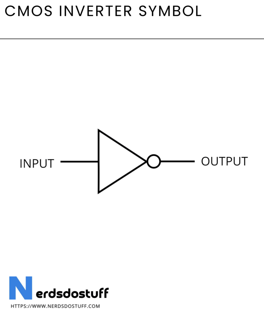
The symbol for a CMOS (Complementary Metal-Oxide-Semiconductor) inverter is a graphical representation used in circuit diagrams to depict its electrical connections and functionality. The symbol typically consists of a triangle representing the complementary transistors (NMOS and PMOS) connected in parallel, sharing a common input and output. Here’s a breakdown of the components in the CMOS inverter symbol:
- Input (IN): The input to the CMOS inverter is represented by a small circle or triangle at the left side of the symbol. This signifies where the input signal is applied.
- Output (OUT): The output is usually shown on the right side of the symbol, opposite the input. It is the point from which the inverted output signal is taken.
CMOS Inverter Circuit
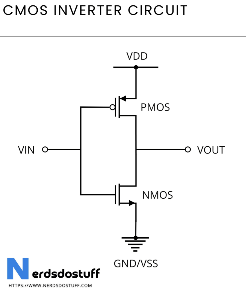
In a CMOS (Complementary Metal-Oxide-Semiconductor) inverter circuit, you have both PMOS (P-type Metal-Oxide-Semiconductor) and NMOS (N-type Metal-Oxide-Semiconductor) transistors working together.
- VDD: This is the positive power supply voltage. It is typically connected to the drain of the PMOS transistor and serves as the high voltage level (logic 1) in the circuit.
- VSS: This is the ground reference voltage, also known as the negative power supply voltage. It is usually connected to the source of the NMOS transistor and serves as the low voltage level (logic 0) in the circuit.
- VIN: This is the input voltage signal applied to the gate terminals of both the PMOS and NMOS transistors.
- VOUT: This is the output voltage signal taken from the common connection (node) between the PMOS and NMOS transistors.
- PMOS Transistor: This transistor is a P-type MOSFET. Its source terminal is connected to VDD (positive supply voltage), its drain terminal is connected to VOUT, and its gate terminal is connected to VIN.
- NMOS Transistor: This transistor is an N-type MOSFET. Its source terminal is connected to VSS (ground), its drain terminal is connected to VOUT, and its gate terminal is connected to VIN.
Working of CMOS Inverter
- Input State (High Voltage – Logic 1):
- When the input voltage (VIN) is at a high level (logic 1), the PMOS transistor conducts, while the NMOS transistor is in the off state.
- The high input voltage turns ON the PMOS transistor because a positive voltage at its gate relative to its source enhances the conductive channel, allowing current to flow from the power supply (VDD) to the output (VOUT).
- At the same time, the NMOS transistor is OFF since a high voltage at its gate relative to its source would create a reverse-biased condition, blocking the flow of current from the output to the ground (VSS).
- Output State (Low Voltage – Logic 0):
- With the PMOS transistor conducting, the output voltage (VOUT) is pulled up towards the power supply voltage (VDD). This creates a logic low (0) at the output because the output voltage is close to VDD.
- The NMOS transistor remains OFF, so there is no current flowing from the output to the ground. The NMOS transistor effectively isolates the output from the ground, maintaining a high voltage.
- Input State (Low Voltage – Logic 0):
- When the input voltage (VIN) is at a low level (logic 0), the NMOS transistor conducts, and the PMOS transistor is in the off state.
- The low input voltage turns ON the NMOS transistor because a positive voltage at its gate relative to its source allows current to flow from the output to the ground (VSS).
- Simultaneously, the PMOS transistor is OFF since a low voltage at its gate relative to its source creates a reverse-biased condition, blocking the flow of current from the power supply to the output.
- Output State (High Voltage – Logic 1):
- With the NMOS transistor conducting, the output voltage (VOUT) is pulled down towards the ground. This creates a logic high (1) at the output because the output voltage is close to VSS.
- The PMOS transistor remains OFF, so there is no current flowing from the power supply to the output. The PMOS transistor effectively isolates the output from the power supply, maintaining a low voltage.
Applications of CMOS Inverter
- Logic Gates:
- CMOS inverters serve as the basic building blocks for various digital logic gates such as AND, OR, NAND, and NOR gates. By combining multiple inverters in specific configurations, a wide range of logical functions can be implemented, forming the basis for digital circuits.
- Flip-Flops and Latches:
- Flip-flops and latches are essential components in sequential logic circuits, commonly used for storing and processing data. CMOS inverters are employed in the construction of these memory elements. The efficiency and low power consumption of CMOS technology make it well-suited for these applications.
- Memory Cells in RAM:
- CMOS inverters play a crucial role in the design of memory cells within Random Access Memory (RAM) circuits. SRAM (Static Random Access Memory) and DRAM (Dynamic Random Access Memory) both utilize CMOS inverters as part of the overall memory cell design, enabling efficient storage and retrieval of data.
- Microprocessors and Integrated Circuits:
- CMOS technology is widely used in the fabrication of microprocessors and other integrated circuits (ICs). The CMOS inverter’s low power consumption and the ability to integrate large numbers of transistors on a single chip make it ideal for designing complex digital systems. The inverters form the basis for various functional blocks within these chips, contributing to the overall performance and energy efficiency of the devices.